1.1 A
Brief History
An integrated circuit (also known as IC, microcircuit, microchip, Silicon chip, or chip) is a single crystal chip of semiconductor containing both active and passive components and their interconnections.
Jack St.
Clair Kilby was an American
electrical engineer who took part in the realization of the first integrated circuit while working at Texas Instruments
in 1958. He was awarded the Nobel Prize in physics in 2000.September 12th
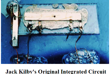
1958 Jack Kilby at Texas instrument had built a simple oscillator IC with
five integrated components (resistors, capacitors, distributed capacitors and
transistors).
 Kilby's invention had a serious drawback, the individual circuit elements
were connected together with gold wires making the circuit difficult to scale
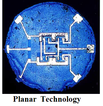
up to any complexity. By late 1958 Jean Hoerni at Fairchild had
developed a structure with N and P junctions formed in silicon. Over the
junctions a thin layer of silicon dioxide was used as an insulator and holes
were etched open in the silicon dioxide to connect to the junctions. In 1959,
Robert Noyce also of Fairchild had the idea to evaporate a thin metal layer
over the circuits created by Hoerni's process. The metal layer connected down
to the junctions through the holes in the silicon dioxide and was then etched
into a pattern to interconnect the circuit.
Planar technology set the
stage for complex integrated circuits and is the process used today. The planar process
is a manufacturing process used in the semiconductor
industry to build individual components of a transistor, and in turn,
connect those transistors together. It is the primary process by which modern integrated circuits are
built.
1.2 Generations
of Integrated Circuit
In
the early days of integrated circuits, only a few transistors could be placed
on a chip, as the scale used was large because of the contemporary technology,
and manufacturing yields were low by today's standards. As the degree of
integration was small, the design process was relatively simple. Over time,
millions, and today billions, of transistors could be placed on one chip, and a
good design required thorough planning.
The integrated circuits can be small
scale integration, medium scale integration, large scale integration, very
large scale integration.
Scale of Integration
The number of
components fitted into a standard size IC represents its integration scale, in
other words it is a density of components. It is classified as follows:
1. SSI – Small Scale Integration:
It has less than 100 components (about 10 gates). SSI circuits were crucial to early aerospace projects, and aerospace projects helped inspire development of the technology.
2. MSI – Medium Scale Integration:
It contains less than 500 components or has more than 10 but less than 100 gates. They were attractive economically because while they cost little more to produce than SSI devices, they allowed more complex systems to be produced using smaller circuit boards, less assembly work (because of fewer separate components), and a number of other advantages.
3. LSI – Large Scale Integration:
Here number of components is between 500 and 300000 or have more than 100 gates. Integrated circuits such as 1K-bit RAMs, calculator chips, and the first microprocessors, that began to be manufactured in moderate quantities in the early 1970s, had under 4000 transistors. True LSI circuits, approaching 10,000 transistors, began to be produced around 1974, for computer main memories and second-generation microprocessors.
4. VLSI – Very Large Scale Integration:
It contains more than
300000 components per chip. In 1986 the first one megabit RAM chips were
introduced, which contained more than one million transistors. Microprocessor
chips passed the million transistor mark in 1989 and the billion transistor
mark in 2005.The trend continues
largely unabated, with chips introduced in 2007 containing tens of billions of
memory transistors.
1.3 Moore’s law
The law is named after Intel co-founder Gordon E. Moore, who described the trend, in his 1965 paper. The paper noted that the number of components in integrated circuits had doubled every year from the invention of the integrated circuit in 1958 until 1965 and predicted that the trend would continue "for at least ten years". His prediction has proven to be uncannily accurate, in part because the law is now used in the semiconductor industry to guide long-term planning and to set targets for research and development.
Moore's law is the observation that, over the history of computing hardware, the number of transistors on integrated circuits doubles approximately every two years. The period often quoted as "18 months" is due to Intel executive David House, who predicted that period for a doubling in chip performance.
1.4 Silicon –The
Starting Material of Integrated Circuit
Silicon is one of nature's most useful elements.
Silicon is the material most commonly used for the manufacturing of
semiconductors. Silicon, as a pure chemical element, is not found free in nature.
It exists primarily in compound form with other chemical elements. In all of
its various forms, silicon makes up 25.7% of the earth's crust, and is the
second most abundant element in the periodic table of elements. It is exceeded
only by oxygen. Silicon occurs chiefly as a compound of silicon and oxygen
called an oxide or as a compound of silicon and salts called a silicate. Silicon
in the form of an oxide most commonly occurs as silicon dioxide, SiO2,
generally called silica, or sand. Other common forms of silicon dioxide are
quartzite, quartz, rock crystal, amethyst, agate, flint, jasper, and opal.
Silicon is preferred over germanium due to following reasons:
- Si devices can operate up to 150 degree Celsius as compared to 100 degrees for Ge
- Si grows a stable oxide (silicon dioxide) which is important in the fabrication of IC as compared to Ge oxide which is unsuited for device applications.
- Ge is more costly than that of Silicon.
- Undoped resistivity of germanium in 47 ohm-cm as that of 23x104 for Si, due to which high voltage rectifying devices are practical with silicon.
- Ge is difficult to dope as compared to Silicon
- Silicon is easily available near the sea beach as a raw material for silicon wafer preparation.
- Growth of silicon oxide layer does not any special arrangements, whereas for growing Ge oxide, special plant has to be installed which increases the cost of the finished product.
- Ge has high junction leakage current or reverse current as compared to that of silicon.
1.5 Integrated Circuit Manufacturing Process Roadmap
The impact of
integrated circuits on the electronics industry has been phenomenal. Not only
are they changing the physical appearance and modes of operation of electronic
equipment, but are also causing major changes in the entire structure of the
electronic industry. Methods of transacting business are changing. The
supplier-user interface is changing. The decision to custom design ICs or use
standard or semicustom devices becomes a major consideration for many electronic
companies.
The
IC manufacturing process roadmap is illustrated in Figure.
The logic designer
can either work for a systems company or be part of the IC design team within
the semiconductor manufacturer. The circuit designer generally works for the
semiconductor manufacturer.
The circuit designer translates the logic
designer's requirements into a semiconductor circuit design. The circuit
designer will convert the electrical schematic of the circuit into the physical
size of each component, i.e., transistor, diode, resistor, capacitor, etc.,
that makes up the circuit. The designer uses a workstation (CAD) to accomplish
the design and do the many different simulations required for design
verification.
The geometrical layout is the
final output of the workstation in the form of a database tape. The database
tape is the input information for the electron-beam system. The electron-beam
system uses the input data to create the reticles or masks required in IC
manufacturing. The number of reticles or masks is determined by the actual
manufacturing process cycle. This is often referred to as the "Fab
Process." The newer Fab Processes use between fourteen and twenty-four
reticles or masks. The central region of Figure depicts the wafer Fab process.
After the wafer Fab process is completed, the wafers are tested electrically to
the required specifications and then forwarded to the assembly process.
The assembly process will package
each electrically good die. After packaging is completed, the device will be
given a final electrical test, burn-in as required and shipped to the end user.
The end user creates the electronic system by bringing together all the
necessary electrical components, mechanical hardware and the final package of
the product.
There is no doubt the world is in
the silicon age. Silicon devices in the form of discrete products or ICs touch
our lives in many ways every day. And — since silicon is the second most
abundant element in the earth, there doesn't appear there will ever be a
shortage of the raw material.
ANEESH P THANKACHAN
M. E (Communication Systems)
B. Tech (Electronics & Communication Engineering)
Engg. Diploma (Applied Electronics)
Associate Professor , Department of ECE
B. Tech (Electronics & Communication Engineering)
Engg. Diploma (Applied Electronics)
Associate Professor , Department of ECE
Younus College of Engineering & Technology, Kollam


Very informative blog. Thanks for sharing with us. Keep sharing.
ReplyDeleteBuy Desktop Resistive Touch Monitors